


Why it matters: HBM3E chips are projected to become a market staple, with demand expected to surge through 2027. Growth will be fueled by generative AI and high-performance computing, both of which require advanced memory solutions to efficiently manage large data volumes. As demand intensifies, so will the competition to supply these chips to Nvidia. Samsung is positioning itself to replace SK Hynix as its primary supplier, and its efforts were recently rewarded with Team Green’s approval of its eight-layer chips.
Samsung Electronics’ eight-layer HBM3E chips have been approved by Nvidia for use in its artificial intelligence processors, marking a significant achievement as Samsung seeks to catch up with SK Hynix in the supply of advanced memory chips for AI applications. According to three sources who spoke to Reuters, Samsung’s eight-layer HBM3E chips successfully passed Nvidia’s tests.
Although the approval is a major milestone, Samsung and Nvidia have not yet signed a supply agreement. However, it is anticipated that such a deal will be finalized soon, with supplies expected to commence by the fourth quarter of 2024.
The approval of Samsung’s HBM3E chips provides Nvidia with an additional supplier for high-bandwidth memory, potentially reducing dependency on a single source and mitigating risks associated with supply chain disruptions. This development also sets the stage for future collaboration between Nvidia and Samsung, which could lead to further advancements in AI processor technology.
Despite the progress with the eight-layer chips, Samsung’s 12-layer version of the HBM3E chips has not yet passed Nvidia’s tests. According to Reuters, this may be due to unresolved issues related to heat and power consumption, which Samsung has been addressing, though Samsung has denied these claims.
This report contrasts with an earlier story from South Korean media outlet Alphabiz, which suggested that Samsung is set to exclusively supply the 12-layer HBM3E to Nvidia. The report indicated that Nvidia CEO Jensen Huang endorsed Samsung’s 12-layer HBM3E product by leaving his signature “Jensen Approved” on a physical unit, signaling Nvidia’s acknowledgment of Samsung’s HBM3E technology.
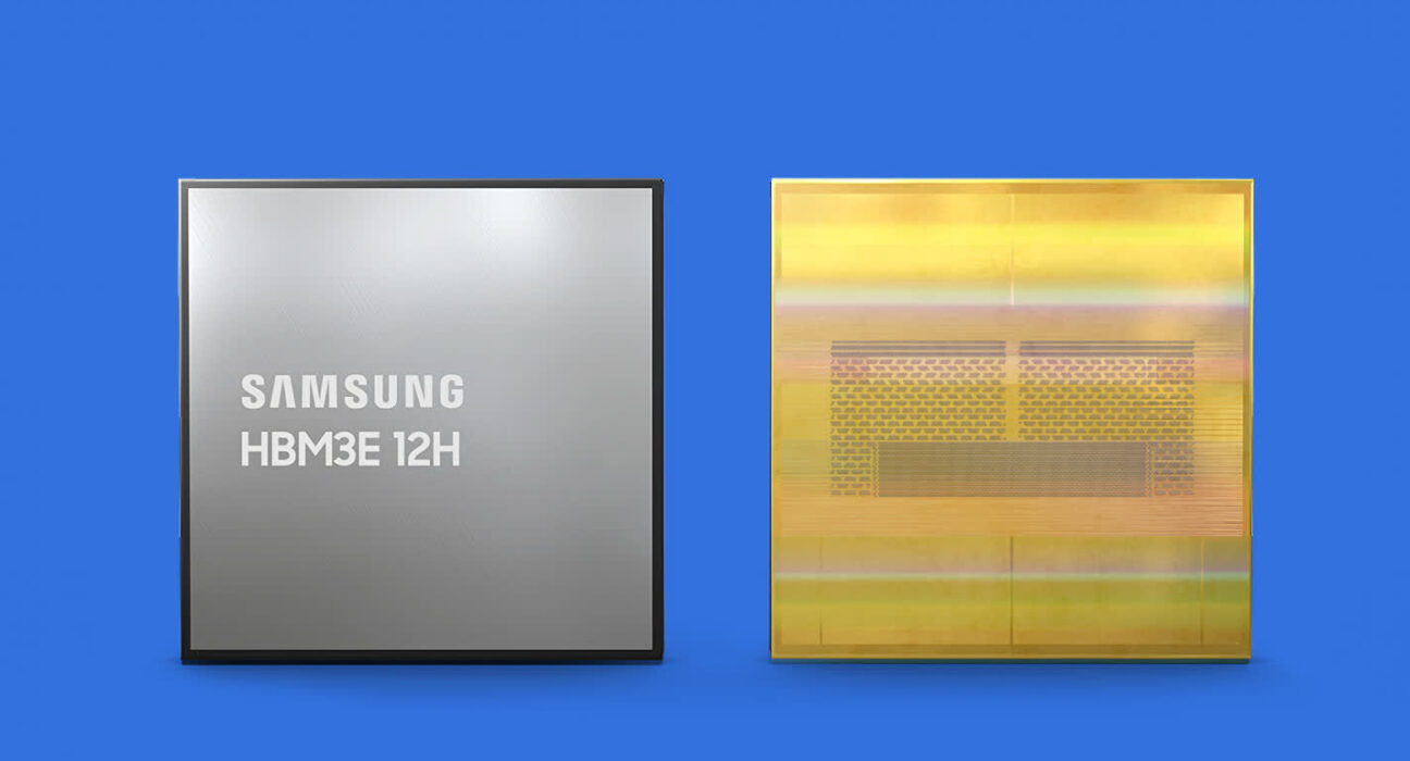
Introduced earlier this year, Samsung’s 12-layer HBM3E chips are more advanced, offering a 50 percent increase in both performance and capacity compared to the eight-layer stack. They also provide a 34 percent increase in average speed for AI model training.
Samsung achieved the 12-layer stack by utilizing advanced thermal compression non-conductive film, maintaining the same height specification as the eight-layer chips, which meets current requirements for HBM memory packaging applications.

According to research firm TrendForce, HBM3E chips are likely to dominate the market in the latter half of the year, reflecting their increasing importance and adoption in the industry.
As Samsung continues to develop its HBM3E technology, it will be competing with SK Hynix, which has been supplying HBM3E chips to Nvidia since late March and holds a strong position in the market. Micron Technology, which has announced plans to supply Nvidia with HBM3E chips for its H200 Tensor Core GPUs, is another key player in this space.
SK Hynix estimates that demand for HBM memory chips will increase at an annual rate of 82 percent through 2027. Meanwhile, Samsung forecasted in July that HBM3E chips would account for 60 percent of its HBM chip sales by the fourth quarter.